William FOGAL
Charge-Barrier Transistor
Charge-Barrier Transistor
Fogal Transistor -- The Truth Behind Charged Barrier Technology
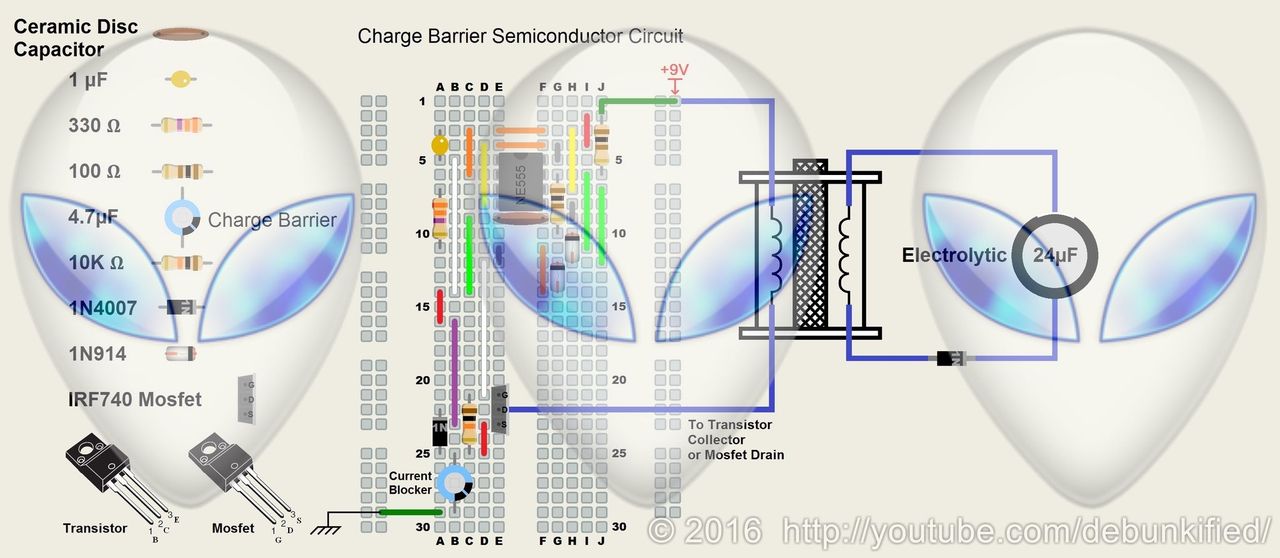
Fogal's Charge Barrier Breadboard Layout
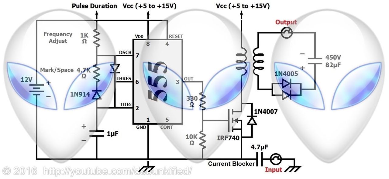
Fogal's Charge Barrier Schematic
Fogal's Charge-Barrier Semiconductor
On The Fogal Transistor -- Commentary and Analysis by Tom Bearden
US5430413 -- High gain, low distortion, faster switching transistor
US5196809 - High gain, low distortion, faster switching transistor
US5311139 - Fuse checker for testing integrity of a miniature, plug-in fuse while the fuse is installed in an electrical circuit
https://svpwiki.com/Fogal-Transistor
Fogal Transistor -- The Truth Behind Charged Barrier Technology
Bill Fogal (1997)
With Special Commentary and Analysis by Colonel Tom Bearden (Retired U.S.Military Officer, Nuclear Physicist)
Introduction
"We are only bound by the limits of our own imagination." We perceive what we cannot see. We feel what we cannot hear. We strive for perfection in our thought models, but we seem to forget that sometimes it is the imperfections in nature that can help to make things work.1
This paper covers a new way of thinking in solid state physics. Now one seeks to utilize and tame pure energy flow rather than just broadly dissipating the collected energy by means of electron current flow. The paper also looks at some of the ideas and theories that make up our world. The Fogal semiconductor - which is an experimentally demonstrated device - may force us to ask some unique questions about conventional EM theories and wonder, "Do things really work that way? Could they work differently after all?"
We particularly caution the reader against simply assuming normal EM theory, either classical or quantal, as having the "final answers." The topology of these models has been severely and arbitrarily reduced. If one looks at circuits in a higher topology algebra, many operations are possible, though excluded from present tensor analysis.2
Energy Flows Continuously from Magnetic and Electric Charges
Have you ever taken two magnets and held one magnet in each hand, with the magnets facing each other with the same poles? As you bring the magnets close to each other, you can feel the repulsion and the build-up of the"energy field" as the magnets begin to push your hands away from each other. Each of the magnetic poles is pouring forth hidden energy3 that acts upon the other pole, producing the force that you feel.
That energy is continuously flowing from the magnets, 4, 5, 6 and fills the entire space around them, literally to the ends of the universe. The electron7 also has such a flowing energy field, and electrons will react just like the magnets under certain conditions. When two like charges approach each other, their streams of energy impact one upon the other, and produce
(i) excess pileup of energy8 on the electrons, and (ii) mutual repulsion.
However, unlike the magnets, usually the electrons are notoriously free to move. So free electrons will rapidly move away from the site of repelling charges. As electrons mutually repel each other and move away, they also drain away the collected portion9 of their excess energy field in the process.10
Now if we could only collect and use the energy from the flowing energy field directly, further down the circuit, and not move the repelling electrons themselves! In that case our constrained electrons would continue to be an inexhaustible source of that energy flow, and we could collect and use the excess energy from them, without draining away the source by allowing electron current flow from it.
And there'd be another great advantage: We would also rid ourselves of most of the electron collision noise, that is created in the lattice by the longitudinal movement of the electrons as ordinary current. In other words, we could simply use the direct energy flow changes caused by our signal modulations, without adding lots of little unwanted and spurious field changes due to those electron collisions. This notion is simple: Use field energy flow to bypass the blocked electron flow, and you bypass much of the noise in the intervening transmission line and associated circuits.
Some Simply Addressed But Advanced Content
To fully comprehend some of the content of this paper, a fairly extensive knowledge of quantum solid state physics is helpful. Even then, using the tantalum electrolytic capacitive material to form and sustain spin density waves at room temperature, and forming an EM field by moving and overlapping the energy states of compressed electrons, appear to be new areas in solid state physics. This paper will also explain why the AC Josephson tunnel junction effect can be developed at room temperature in the charged barrier device, and how and why the AC supercurrent can also be developed at room temperature.11
Design, Components, and Functions
Let's Take a Look at the Basic Design
The simplified schematic of the hybrid charged barrier semiconductor is shown here in Figure 1:
The device has an electrolytic capacitor and a parallel resistor attached to the emitter junction of a bipolar transistor. Such a circuit configuration has been known in textbook theory as a bypass element and the capacitor in the circuit configuration will react to frequency to lower the emitter resistance and create gain. However, there is one interesting point to consider. I have been granted two U.S. Patents on the same circuit configuration, using an electrolytic capacitor to form a unitary structure. Under certain conditions, electrolytic capacitors react differently in this type of circuit configuration than a standard non-electrolytic bypass capacitor.
I use the electrolytic capacitor to create a unique electromagnetic field.The parallel resistor is used to "bleed-off" excess charge potential from the plate of the capacitor to generate the electromagnetic field. It also performs another function we will detail later. The exact values of the capacitive element and resistive element are not listed at this time.
Let's Look at Capacitors
In theory, a simple capacitor will pass an AC signal and voltage and block a DC voltage from crossing the plate area. However, a physical capacitor is not necessarily simple; instead, it is a complicated system having many internal functions. An electrolytic capacitor will pass an AC signal and voltage, and also hold a DC charge - with its accompanying DC potential - on the plate area of the capacitor.12 If an electrolytic capacitor can hold a DC charge potential on the plate area, then one can move small portions of that charge potential and that charge, with the use of a parallel bleed-off resistor. This small bleed-off current and change of E-field will create a very small, associated magnetic field on the plate area of the capacitor. Through experimentation it has been found that this very small electromagnetic field will oscillate at a very high frequency that is not detected under normal test conditions.13
Conventional theory has shown that one needs to have a movement of the charge state to generate current to create a magnetic field.14 However, theory does not tell the exact amount of current needed to create the field. Could the bleed-off effect from a parallel resistor element change enough of the charge state to sustain a very small EM field? The resistor element would have to have just the right specific value in order to bleed-off just enough excess charge potential, so that the charge state between the plate of the capacitive element and the resistor bleed-off would not reach a point of equilibrium (equalization) between the charge states.
Scope Traces
At the point of charge, with no signal applied, and with a bias of the junction, the capacitive element will charge to the voltage potential of 250 mV DC at the emitter junction. The parallel resistor element will work to "bleed-off" excess charge from the capacitor plate area, and try to reach a point of equalization of the charge state. However, the associated field will oscillate at a frequency around 500 MHz and will not reach a point of total equalization due to this high frequency oscillation. In other words, equilibrium does not occur.15
Formation of Electromagnetic Field
Figure 2. The formation of the electromagnetic field is shown in Figure 2, which is a photograph from a Tektronix transistor curve tracer operating in the microamp region. A reading of the DC operating voltage of the emitter junction of the transistor will not show a change in the voltage potential due to the high frequency oscillation of the electromagnetic field. At this point, the emitter electrons become trapped and pinned within the electromagnetic field of the capacitor. This pinning blocks current and dampens the amount of electron collision noise and heat due to electron interaction.16
Charge-Blocking and Formation of the AC Supercurrent
Figure 3.The photograph in Figure 3 is taken from the Tektronix transistor curve tracer operating in the microamp region. At the point of a small signal injection to the base region of the transistor, the effect of the AC carrier disruption to the internal DC emitter junction electromagnetic field can clearly be seen. This effect is caused by the Overpotential of Charge State and the compression of the pinned electron clusters within the DC charged electromagnetic field developed by the capacitor. At this point in device conduction, the parallel resistor element will try to equalize the field charge, and align the pinned electron clusters in the charged field on the capacitor plate. The E-field will start to develop along with its associated Poynting energy density flow (S-flow).17
Formation of the AC Supercurrent
Figure 4. The photograph in Figure 4, taken from the Tektronix transistor curve tracer, shows the effect to "disruption and compression of the pinned electron clusters." At this point in time, in the semiconductor the parallel resistor element can no longer handle the bleed-off of excess charge potential from the charged plate of the capacitor, due to the compression of electrons and the consequent rapid formation of an E-field. So there is a buildup of the Poynting energy density flow due to the change in electron energy state and compression of charge clusters. A spin density wave will develop and increase within the tantalum capacitor.18
Discharge of the AC Supercurrent
Figure 5. The photograph in Figure 5, again taken from the Tektronix transistor curve tracer, shows almost the full development of the AC supercurrent, due to the Poynting energy density flow and the increased spin density wave action of the tantalum capacitor. The development of the E-field is almost complete. The emitter junction DC electromagnetic field is about to collapse and release the AC supercurrent as well as the flow of Poynting energy density. The AC supercurrent is too massive and the increased nature of the spin density wave of the tantalum element is too fast, due to the buildup of the E-field, for the bleed-off resistor to effectively regulate and shut down the action.19
Poynting Energy Flow
Figure 6. Taken from the Tektronix transistor curve tracer, the photograph in Figure 6 shows the point of discharge and the Poynting energy density flow, the AC supercurrent, and the collapse of the DC charged electromagnetic field, due to the change of energy state on the plate of the tantalum capacitor. Most of the device conduction is a Poynting energy density flow across the doped regions of the device's crystal lattice. With a dramatic decrease in electron collisions, the S-flow now is not subject to distortions due to the material defects within the lattice structure. Device switching times are far faster (at optical speed) and there are few if any limitations on frequency response.
The phenomenal frequency response - up to essentially the optical region - follows, since the shortest frequency wavelengths can be passed directly as Poynting energy density flow.20 Without divergence or scattering of this energy flow, there is no "work" being done in the conventional sense on the non-translating electrons in that region, even though they are potentialized. That is, electron transport has been halted temporarily or dramatically reduced, while the Poynting flow continues apace. With most electrons not being translated longitudinally, there is no heat build-up in the device as there is with lattice vibration interactions with a normal electron current.21 This device can work as a charge coupled device22 with the ability to pass both voltage and Poynting current flow S rather than conduction electron current flow dq/dt.23
Researching Charge and Poynting Flow in Circuits
Tom Bearden is a very good friend of mine in Huntsville, Alabama. Tom has been deeply involved in research for a number of years to explain and define the charge state in physics. He has taken a serious look at the flow of Poynting energy in circuits,24 and how most circuit analysis focuses on the power (rate of dissipation of the energy flow) in circuits rather than on the actual rate of energy transport flow (which is not power at all, if it is not dissipated). Tom can explain the basic theory for formation of the charge state25 and he can explain the Poynting energy flow used in my charged barrier technology.26 The reader is referred to the extensive endnote comments added by him. Over the last few years it has been a real pleasure to exchange ideas with him.
Remember the Magnets
Tantalum is one of the elements that is used in the construction of the charged barrier device, as well as the "parallel resistor element." Under certain conditions, when stimulated with a very small electric current to align the charge state, the excess bleed-off effect due to the parallel resistor can move the charge state on the capacitor and develop a very small electromagnetic field. Electrons are "held" and "pinned" within thisfield to reduce electron lattice interaction within the emitter junction.
With the influence of the AC conduction electrons reacting with the pinned electrons within the charged field, a unique effect will start to happen: The clusters of bound electrons within the charged field are compressed to a point where there is a "change of energy state" within the compressed, bound electrons in the tantalum lattice. This will start the formation of the E-field due to the interaction of the compressed electron clusters with the influence of the AC conduction electrons. Remember the magnets when their like poles were brought within close proximity to each other? An analogous action will start the formation of the AC supercurrentand the Poynting energy flow within the device.27
Charged Barrier Fogal Engine
Putting together all the actions we have discussed, we may compare the electromagnetic actions as the actions of a special kind of engine cycling, as shown in Figure 7.
In Figure 7, we show four analogous actions involved in the "Fogal engine". Figure 7A shows the start of the "down stroke" of the Fogal emitter piston, so to speak, and the formation of the DC electromagnetic field. Figure 7B shows the signal injection into the cylinder from the injector base region, as the emitter piston pulls the signal into the chamber. Figure 7C shows the compression of electron density and the formation of the amplified E-field due to the charge compression, with a resulting expansion of the Poynting energy density flow. Figure 7D shows the point of discharge of the Poynting energy density flow, the resulting AC supercurrent, and the collapse of the DC electromagnetic field of the emitter piston.
Testing the Fogal Charged Barrier Semiconductor
Device Testing Parameters for Tektronix
Now that you have seen the pictures of the formation of the internal DC electromagnetic field and the development of the AC supercurrent, I will explain how to test this device. The Charged Barrier device has certain testing parameters that have to be followed to test it accurately. The device must be operated within certain parameters to maintain the internal electromagnetic field action. Tests have to be constructed on the Tektronix transistor curve tracer in the microamp range of operation, in order to keep from saturating the internal electromagnetic field. Important: The Charged Barrier prototype device will test and look like a normal transistor when tested or operated outside of its specified operating parameters!
In the tests, the testing parameters on the Tektronix were set up as follows: The collector current was set at 20 ½A per division. The base current was set at 0.1 �A with signal injection to the base region. The supply voltage was set at 10 V DC per division. The signal injection was 100,000 kHz (100 MHz) at a level of less than 100 ½VAC. Important: This device cannot be tested on the Tektronix curve tracer equipment in the milliamp range of operation for a normal transistor. Testing it in the milliamp range will overload and shut down the internal electromagnetic field developed by the electrolytic capacitor. The prototype device will then test and look like any normal transistor, with similar noise figure, gain, and frequency range. The "new effects" only occur at the proper microamp range as specified, and only then does one obtain in the Fogal transistor the dramatic noise reduction, increase in sensitivity, increased gain, and increased frequency response as well as "optical" type functioning due to the blocking of dq/dt current flow and the increase in Poynting energy density flow.
Circuit Testing the Device
The Fogal Charge Barrier transistor can be tested under normal circuit conditions with a 3 V DC supply voltage and a bias to the base-emitter junction of 0.7V DC with the emitter grounded. A normal transistor under these conditions will turn on and conduct with an input to the base region of 4.5 mV AC at 0.1 ½A AC, and produce a gain at the collector junction of 20 mV AC with 0.1 ½A of current. Under the same circuit conditions, the Charged Barrier device with a signal injection of 200 ½V AC at 0.1 ½A to the base region, will produce 450 mVAC and an AC current of 133 ½A AC at the collector junction. A large signal injection to the base region of the Charged Barrier device will overload and shut down the internal electromagnetic field and the device will test just like a normal transistor, until a point of device saturation is reached where the device will pass large amounts of current without a noticeable change in device temperature.28 The device can easily be used in existing equipment for signal processing applications to process and reduce the noise content of signals.
Device Wave Function
Though not in conventional theory, signal waves actually travel in wave pairs, 29, 30 each pair containing the familiar wave and an associated "hidden" antiwave. The two waves of the pair have the same frequency. Current semiconductor technology cannot separate these wave pairs, due to limitations in switching time.31 The Charged Barrier device can switch at a sufficiently fast rate to:
(i) separate the wave pairs at the higher frequencies and (ii) define the "polarization of light waves" to show background imaging and enhanced video resolution.
A pre-recorded audio or video tape can be processed to reveal hidden sounds or background imaging that standard electronic equipment will not process.32 The device has been shown to process frequencies in the range from 20 Hz to 5 GHz and higher with no loss in frequency response, due to the ability of the device to separate and process wave pairs, and due to faster device switching.
Some Foreseeable Applications
Charged Barrier Applications
Prototype Charged Barrier devices have been tested in video equipment to process composite video images for a higher resolution. The device has the ability to process and separate the wave pairs and define the "polarization" of light from background objects. This ability can produce a high definition image on a CRT, and a near-holographic image on liquid crystal display panels. The clarity of liquid crystal display panels can be greatly improved by the switching speed of the Charged Barrier technology, with the visual improvement sometimes being startling.
Novel Encryption and Transmission Capability
A preliminary test was constructed in Huntsville, Alabama in May of 1996 to determine if video information could be infolded within a DC voltage potential and transmitted across a wired medium.33 Live video information at 30 frames per second was processed and converted by full wave rectification into a DCp otential at a voltage of 1.6 V DC and connected to a twisted pair wire medium of 2,000 feet in length. As a voltage, the 5 MHz video information rectified to DC potential had no modulation or AC signal present that could be detected by sensitive signal processing equipment. The analog oscilloscopes that were used to monitor the transmission could only see the DC voltage flat line, although the best digital storage scope could see very weak signal residues because of slightly less than 100% filtering. I later performed additional tests with increased filtering, so that the residues could not be seen. These tests were constructed to see if video information could be "infolded" into an audio carrier and transmitted across an ELF frequency transmission source for communication with submarines, or down a 2,000 ft twisted wire pair. The Charged Barrier device was able to process the hidden video, due to the ability of the device to sense the infolded AC electromagnetic wave information hidden inside the rectified DC voltage, sensed as a disruption to the internal DC electromagnetic field of the Charged Barrier device. Using the Fogal semiconductor, a good video image was shown on the monitor at the end of the wired medium. The Huntsville test was considered encouraging. As stated, I have since repeated the test with a better buildup, to eliminate the very weak signal residues, and the effects are real and replicable. Use of the "infolded" EM waves in an ELF carrier for video frequency signaling is real.
A novel effect uncovered in the Huntsville tests was that, by adjusting the gain control of the receiving box containing the charged barrier device, the focused field of view of the fixed image could be varied, even though no adjustment at all was made in the video camera's stationary focusing. This showed that the "internal information" in an image actually contains everything needed to scan a fixed volume of space, forward and backward in radial distance, in a focused manner. The internal information seems to contain information on the entire volume of view of the camera.34 And it is possible to scan that volume, from a seemingly "fixed" image where much of the image is "out of the camera-focused field of view). The implications for photo analysis are obvious and profound.
The Charged Barrier device, once precision prototypes are available, can be utilized to encode signals within signals, similar to wavelet technology, or within voltage. Transmissions of such infolded signals could not be detected by conventional signal processing equipment without first being processed by a Charged Barrier device. Without the need for fiber optic cable, conventional wired telephone or cable networks and high voltage AC transmission lines could be used as a transmission source without the need for line amplifiers or noise cancellation equipment. There would be essentially no bandwidth limitations, once the technology is developed.
Future Charged Barrier Applications
Existing radar technology can be refined and improved with the Charged Barrier device. One of the most complex problems in the industry is the "noise content" in signal processing. The Charged Barrier device can be used as a front end low noise amplifier and increase the sensitivity of the target signature scan capability. Radar imaging could be greatly improved simply by processing the return image with the Charged Barrier device for high resolution CRTs and liquid crystal display panels. Systems could also be improved for faster targeting and return echo due to the optical speed of the Charged Barrier device switching. By utilizing the"internal" information, it should be possible to develop improved imaging for sonar applications, so there will be no gaps in the frequency spectrum. The ability to "get at" and detect the hidden internal EM information of an object from its surface reflection, is an innate capability of the Charged Barrier device that needs to be explored. It is already well-known that the entire interior of a dielectric participates in the reflection of light from it; the information on the interior of the reflecting object is in the reflected image, but in the form of hidden EM variables.
New Type of Radar and Sonar Imaging Application
A new type of "volume viewing" radar system can be constructed with the Charged Barrier Technology that can scan the "inner EM signal image" produced over a given area or volume, sensing disruptions within the earth's magnetic field. The movement through that volume of an object -such as a low-flying aircraft made of metal or epoxy resin skin design - can be detected and tracked, regardless of electronic counter measures andatmospheric disruptions such as tornadoes, hurricanes, or wind shear due to microbursts, without the need for target echo return capability. The Charged Barrier device can sense and amplify very small disruptions to the "internal" electromagnetic fields and create an image for identification. The volume can be scanned "in focus" back and forth in distance.
For sound direction and distance sensing, the pinna (small folds) of the outer ear use phase reflection information more than 40 dB below the primary sound signal that strikes the eardrum.35 Any target's nonlinearities and defects, regardless of overall reflective angle and reflective sonar signals, also produce such minute, hidden "pinna" phase reflections and disturbances in:
(i) sonar reflections, (ii) the Earth's magnetic field (and in fact in the electric field between the surface of the Earth and the electrosphere), and (iii) in the ocean, in the overall subsurface static potential formed by the conglomerate potentials of the hydrogen bonding, ionizations, etc.
These "pinna" signals are broadcast through the surrounding normal fields/potentials of the Earth, including underneath the ocean, although they are many dB below the normal field fluctuations whose gradients are detected by normal sensors. By detecting this "internal" information, Charged Barrier detectors would be able to detect these hidden "pinna" signals and dramatically increase the information available to the sensor system. Terrain-following cruise missiles, for example, could be detected, tracked, and identified by this means, as could submarines, floating subsurface mines, etc. Field camouflage and decoying would be essentially useless against such sensors.
Adaptation of Such "Radars" to Specialized Sensing
If sufficient of the "pinna" signals can be detected and utilized, a totally new method of internal target identification and discrimination - as well as typing and identification of the internal warhead(s) and other components on board the target - could be developed using the Charged Barrier technology. From the pinna signals, decoys and ECM-generated "false returns" could readily be discriminated from the real targets.
Specialized detection devices for airports could be developed that would utilize the pinna information to easily and cheaply detect and identify the contents of packages, luggage, etc. This would provide enhanced security against terrorist bombs, weapons, drug smuggling, etc.
Of particular usefulness would be the development of "pinna scanning" sensors which could peer beneath the ground's surface, detecting mines, tunnels, etc. Identification and classification of the detected subterranean objects and their interior contents is also foreseeable.
Induction of Forces and Patterns of Forces In Atomic Nuclei
A force-free (gradient-free) scalar potential readily penetrates the electron shells of the atom, penetrating directly to the nucleus and interacting with it. By infolding desired E-fields and B-fields inside the scalar potential (inside pure DC voltage), one can insert desired electromagnetic forces - and control their magnitude, direction, frequency, and duration - directly inside an atomic nucleus. At least in theory, by sustaining and manipulating these forces in the nucleus, the atomic nucleus itself is subject to direct manipulation and engineering, as contrasted to the present practice of "firing in a bullet" such as a neutron to get through the electron shell barriers and produce limited nuclear effects. It may be that eventually such an electromagnetic nucleus-engineering approach, made possible by Charged Barrier technology, can be utilized to render harmless the steadily accumulating radioactive wastes around the world.
Reduction of Drag on Vehicle Skins
Another application also looms for the use of the charged barrier technology. This application is for the reduction of the drag of the medium on vehicle skins. My preliminary tests on model boats in water have demonstrated the effect to exist and operate, though more definitive tests are called for.
Basically the molecules or atoms of the medium, in contact with the skin of a moving vehicle, create a boundary layer of dense matter which exerts frictional drag forces on the skin to retard the forward movement. Because of the use of phase conjugation and Poynting flow, rather than pure current dq/dt flow, the charged barrier technology can be used to charge the skin of the vehicle in a peculiar fashion. The tiny nonlinearities of the skin become pumped phase conjugate mirrors (considering the internal electromagnetics of the static charge, where the hidden biwaves comprise the pumping). Let us consider such a charged skin as now containing a series of pumped phase conjugate mirrors (PPCMs). The incoming atoms or molecules of the medium comprising the boundary layer do possess asymmetrical charge volumes, and so they produce "signal wave" inputs to the PPCMs as they come in. With a good charge on the PPCMs, their hidden biwave pumping is substantial. Consequently the PPCMs emit highly amplified antisignals - phase conjugate replica waves (PCRs). By the distortion correction theorem, these highly amplified antiwaves backtrack precisely to the incoming asymmetric charges, where they interact to produce force fields that repel them.36 The point is, there is no recoil on a pumped phase conjugate mirror (PPCM), when it emits such a highly amplified PCR. This is already a theoretical and experimental fact in nonlinear optics. So there is no consequent Newtonian third law recoil force back on the PPCMs comprising the skin of the vehicle.
In short, one has produced a deliberate "pinpoint, repelling force field" upon each of the incoming atoms and molecules of the medium, without any matching recoil force upon the moving vehicle. Better, all the energy in the force field is concentrated only upon the targets, rather than distributed uniformly in space along wave fronts. The end result is to dramatically reduce or lower the boundary layer, without any drag force reaction being exerted upon the vehicle by that operation. This significantly reduces the skin drag and increases the speed of the vehicle through the medium, for a given on-board propulsion force.
Application of this new kind of "smart skin" technology is straightforward. It should allow ships that increase (even double) their velocity through water for the same expenditure of propeller energy. It should enable super-fast torpedoes, perhaps in the 200 to 300 nautical miles per hour range.
Extended Application of Induced Forces at a Distance
In theory, the "pinpoint" application of force upon a distant target, by self-targeting processes, is not limited to the small distance required to prevent formation of much of the skin boundary layer. Instead, the self-targeting effect can be extended. Our space-borne laser research and development, for example, called for using iterative phase conjugate shooting and self-targeting to hold a laser beam locked on the same spot on a rising hostile booster, up to 10,000 miles distance, providing dwell time for the laser to burn through the casing and destroy the booster during its launch phase.
Follow-on generations of development should add the capability of pinpoint repulsion by an attacked ship of incoming hostile torpedoes, shells, missiles, etc. It should enable faster aircraft, with reduced fuel consumption. In large buildings it could conceivably be applied to lower the resistance of the ducting to the passage of heated or cooled air. In heat pumps it should also increase the COP past the present theoretical8.22 limit, by dramatically reducing the drag exerted by the gases being compressed and pumped.
With use of the pinna information, scanning the ocean's surface can detectand track submarines lurking in the ocean's depths. Literally the oceans can be made "transparent" in a specialized sense.
There are many other applications for the charged barrier technology; the above examples simply serve as "for instances" to tickle the imagination.
In Summary
As can be seen, the advent of Charged Barrier technology and its further development offers a breathtaking extension of present electronic technologies.
Dramatic new capabilities emerge in military defense, to provide for the security of our nation, our armed forces, and our civilian population.
In astrophysics, the detection and use of the "pinna" information could provide unparalleled details on the internal mechanisms, structures, and constituency of planets and stars.
In geophysics, the "pinna" information could provide unparalleled details on the layers, structures, constituents, faults, etc. of the earth underneath the surface. Again, in a specialized sense the earth is made "transparent."
In medicine, the "pinna" information contained within the weak EM emanations from the body would provide details on structures, cellular disorders, infections, and other irregularities within the body, including organs. Eventually a comprehensive diagnosis of the entire body and its cellular functions could be provided by externally scanning the pinna hidden-variable "information content of the field."
In biology the pinna information could provide unparalleled insight into the details and functioning of the brain, its different layers and structures, and of the nervous system. Further, pinna information could reveal the structuring and functioning of the body's recuperative system, as contrasted to the immune system. Very little is presently known about the recuperative system, which is usually just "assumed" by medical scientists.
Conclusion
Just as the microscope opened up a previously hidden microworld and its dynamics, the Charged Barrier technology will open up a previously hidden "internal" hidden variable electrodynamic world that will enlarge every present electronic field of endeavor.
Long ago a great scientist, Max Planck,37 said:
"An important scientific innovation rarely makes its way by gradually winning over and converting its opponents: it rarely happens that Saul becomes Paul. What does happen is that its opponents gradually die out, and that the growing generation is familiarized with the ideas from the beginning."
Arthur C. Clarke38 characterized the four successive stages of response to any new and revolutionary innovation as follows:
"It's crazy!
It may be possible - so what?
I said it was a good idea all along.
I thought of it first."
The Aharonov-Bohm effect, predicted in 1959, required nearly 30 years after its 1960 demonstration by Chambers until it was begrudgingly accepted. Mayer, who discovered the modern thermodynamic notion of conservation of energy related to work, was hounded and chastised so severely that he suffered a breakdown. Years later, he was lionized for the same effort! Wegener, a German meteorologist, was made a laughing stock and his name became a pseudonym for "utter fool," because he advanced the concept of continental drift in 1912. In the 1960s the evidence for continental drift became overwhelming, and today it is widely taught and part of the standard science curriculum. Gauss, the great mathematician, worked out nonlinear geometry but kept it firmly hidden for 30 years, because he knew that if he published it, his peers would destroy him. In the 1930s Goddard was ridiculed and called "moon-mad Goddard" because he predicted his rocketry would carry men to the moon. Years later when the Nazi fired V-1 and V-2 rockets against London, those rockets used the gyroscopic stabilization and many other features discovered and pioneered by Goddard. And as everyone knows, rocketry did indeed carry men to the moon. Science has a long and unsavory history of severely punishing innovation and new thinking. In the modern world such scientific suppression of innovation is uncalled-for, but it is still very much the rule rather than the exception.
The Charged Barrier technology is an innovation which calls for using the energy flow in circuits that is already
(i) extracted from the vacuum flux and (ii) freely provided to the external circuit by the source dipoles.
It utilizes an extended electromagnetics that includes a higher topology and a new, inner "hidden variable" EM. This "inner EM" has been in the literature for nearly a hundred years, but ignored. The use of the charged barrier technology will expose many of the present shortcomings in EM theory and models, but it should also lead to a corrected, highly extended electromagnetics.
Now that you know the theory behind how this technology works, be aware you still need the exact design parameters and component tolerances in order to duplicate the technology.
Let us hope that the charged barrier technology can receive the full scientific attention, testing, and theoretical modeling that it deserves. With that attention and examination I believe my technology will usher ina new revolution in electronics.
https://www.youtube.com/watch?v=HFH_8yGgS10
Fogal's Charge Barrier Semiconductor
This is a replication of the Fogal Charge Barrier Semiconductor. The idea is to let the voltage through or dielectric (information) before current begins to flow. To me this is what a Tesla spark gap is doing in a round about way. Tom Bearden has written about this type of thing in detail and refers to the Fogal Charge barrier.
https://goo.gl/YZAtfD
Fogal's Charge Barrier Breadboard Layout
https://goo.gl/VvAg3m
Fogal's Charge Barrier Schematic
https://www.billstclair.com/www.cheniere.org/misc/fogal.htm
Fogal's Charge-Barrier Semiconductor
Fogal's patented semiconductor can be rigged as a true negative resistor also, because it can perform asymmetrical self-regauging, and isolate its source dipole from much of the back emf current flow. It uses time-reversal to accomplish flow of current against the voltage.
The Pauli exclusion principle prohibits one from time-reversing a single fermion (spin 1/2 etc. entity) such as an electron. However, it does not exclude time-reversing bosons or quasi-bosons (spin-1 entities or multiples thereof). You just have to use even numbers of fermions, in order to time-reverse them. Whoever wishes to time-reverse a single electron anyway, in negative resistor power systems? You wish to time-reverse scads of them! So all it means is that you do that in even numbers only. But it's permissible by the laws of physics. So, yes, Fogal cannot time-reverse one electron by itself. But he can time-reverse gobs of them, to give a steady current against the voltage when he so rigs the semiconductor.
Fogal has experienced incredible difficulties in trying to get his patented semiconductor into production. It's a long story, but suffice it to say that multiple government agencies have tried to steal it from him — uh, pardon me, exercise what they euphemistically refer to as "march-in" rights.
Isn't that a neat little thieving, stealing, piracy phrase to put in the fine print of a U.S. Government contract!
So the government has tried to steal Bill's invention from him on several occasions. They even offered him a quite tidy sum of money in grant, if he would just thereby "sell" it to them. Since when do government agencies try to pry away a company's inventions and research fruits? The dastards are supposed to help the company to do further research and development. That's what the taxpayer has charged them with doing. So why are they acting as a bunch of thieves, robbers, and pirates?
Let me enlightenment you about under-the-table agreements. Widespread throughout government contracting there is a sweetheart deal of collusion and graft. It works this way: The government fellow in position to swing the large contracts to a major company, arrives at a personal (off the record, of course!) agreement with his favorite defense contractor. In return for him swinging some lucrative business to that company, then when the government fellow retires, he will go to work for that company as a Vice President with stock options, etc.
So he looks for things to swing to that company, including things he can "seize" under pretext of march-in rights, national security, etc. If he's a good gold digger for the company, it works like a charm. He swings in the gold to them, and he becomes a multimillionaire when he retires.
Could that have been involved in the cases regarding Bill's novel new semiconductor? There is no way to know. I certainly am not making any such allegation! What I'm saying is that this sort of thing is quite often done. It's often the rule rather than the exception. Remember, I worked in aerospace for 17 years. I saw it happen. It's even worse today.
So the question is: Why did these government agencies want to seize Bill's years of work and his patents, for peanuts? We will probably never know for sure. It is just very suspicious that such seizure and takeover language were in those proffered contracts. The burning question is: Why?
My own alma mater — which just happens to have a major government contract in semiconductor work with one of those agencies wishing to obtain "march-in" rights — then offered to help Fogal get his semiconductor into production. Ugh! In the fine print of the proposed contract they produced was a similar clause: All patents would have reverted to the University. Seems like even my own alma mater was greedy and conniving.
A host of vulture capitalists etc. have tried to "take it off his hands". So we'll have to see whether or not he will be able to get it into production. Just now the prognosis is not too good. Of course we're rooting mightily for Fogal, and helping all we can, and we do hope that somewhere there is a legitimate "deal" that isn't downright theft, that will allow Bill's chip to be produced. It will revolutionize several major fields if that ever happens.
I can tell you this. If CTEC ever succeeds, Bill Fogal will be endowed, and his semiconductor will indeed be produced and marketed. And under his own control and his own company.
https://studfile.net/preview/21473698/
On The Fogal Transistor -- Commentary and Analysis by Tom Bearden
1.
One must consider the "imperfections" in our present "smoothed" theoretical models. In attempting to explain the unorthodox functioning of the Fogal semiconductor, we are invoking phenomenology from what would be a higher topological model, or a model which is a superset of the accepted models. It follows that, in the higher topology, many things will become possible that were not possible in the basic "smoothed" model of lower topology.
This is particularly true in electromagnetics, where Maxwell's 20 quaternion equations in 20 unknowns were arbitrarily reduced -- primarily by Heaviside and Hertz -- to a vector set of some four equations (variables separated) or two equations (potential form, variables not separated). In reducing the topology so severely, the present EM model is only a small subset of nature's EM. Further, suppose one performs an EM analysis of a circuit in a higher topology algebra -- e.g., quaternion algebra, which has a higher topology than tensors. We will then find many functions that circuits actually perform, which will not show in even the most sophisticated tensor analysis. For the proof that inventors -- such as Tesla -- sometimes capture and utilize such hyperfunctioning which present electrodynamicists have not comprehended, see:
T.W. Barrett, "Tesla's Nonlinear Oscillator-Shuttle-Circuit (OSC) Theory"
Annales de la Fondation Louis de Broglie, 16(1), 1991, p. 23-41.
For another refreshing look at the far frontiers of still-developing EM theory, see:
T.W. Barrett and D.M Grimes, [Eds.], "Advanced Electromagnetism: Foundations, Theory, & Applications"
World Scientific, (Singapore, New Jersey, London, and Hong Kong), Suite 1B, 1060 Main Street, River Edge, New Jersey, 07661, 1995.
This line of thinking leads to a very useful tool in qualitatively analyzing novel results obtained in experiments with multiple nonlinear components. Barrett, 1991, ibid. shows us that we can expect nonlinear optical functioning of "ordinary-appearing" circuits as one of the primary higher-topology effects that will usually be observed. Hence when one encounters unusual phenomena in novel circuits, one of the first rules is to look for the nonlinear optical functioning of the pieces of the components, at other than optical frequencies. This will often prove to be highly useful, and the primary way to search for the hidden mechanisms involved in higher topology EM functioning beyond the realm of vectors and tensors. Of course, then the results of the qualitative evaluation must itself be evaluated against the hard experimental data for consistency or inconsistency.
2.
See Barrett, 1991, ibid. for the proof. As an example, when charge blocking is applied or partially applied, circuits can often perform optical functions even without the presence of optical materials. From our own work it appears that the hidden variable EM inside the scalar potential -- as shown by Stoney and Whittaker [to be covered later in these notes] -- easily acts in a fashion prescribed by nonlinear phase conjugate optics theory, even when the frequencies are well below the optical region and even in the ELF region.
We accent that it is well-known that there exists radiationless transport of energy between excited and nonexcited atoms, particularly in semiconductors, where in some cases it has been referred to as the interference of reactive EM field components. E.g., see:
A.A. Kolokolov and G.V. Skrotskii, "Interference of reactive components of an electromagnetic field"
Sov. Phys. Usp., 35(12), Dec. 1992, p. 1089-1093.
Speaking of this type of interference, Kolokolov and Skrotskii state, "As a result an interference flux of energy in a new direction is formed, where energy transport for the original waves can be completely absent."
Further, it is now known that extremely large second-order susceptibilities can be obtained in chargeblocking asymmetric quantum wells in semiconductors. This has been predicted to lead to the emergence of new properties in such semiconductors, such as double resonance enhancement, and even fully solid-state parametric oscillators. E.g., see:
E. Rosencher et al., "Quantum engineering of optical nonlinearities"
Science, Vol. 271, Jan. 12, 1996, p. 168-172.
It would appear that the forefront of semiconductor work on quantum wells and charge trapping is groping toward the type of capability already possessed by the patented Fogal semiconductor.
3.
We emphasize that the notion of energy flow through space did not even exist in physics, at the time Maxwell formulated his theory in the 1860s. The concept of energy flowing through space was formulated by Heaviside and independently by Poynting, after Maxwell had already been dead for a decade. Heaviside published first, but not prestigiously. Poynting published not long after, in a prestigious journal. Hence the theory bears Poynting's name, as does the energy flow vector. But Poynting himself credited Heaviside as being first.
The point is, electrodynamicists were already completely focused upon the energy dissipation in a circuit, well before Maxwell developed his theory. Succeeding generations of electrodynamicists
have maintained essentially the same focus in circuits. We produce power (rate of energy dissipation) electrical engineers rather than energy transport engineers.
4.
As is well-known, a magnetic dipole or an electric dipole produces a continuous flow of Poynting energy. What is not included in EM theory is that -- from particle physics, not classical EM theory! -- the dipole is a broken symmetry in the violent virtual particle flux exchange between the vacuum and the charges comprising the ends of the dipole. Since the magnetic or electric charge is a broken symmetry, it is a "gate" that extracts energy from the vacuum, and it also produces something observable (the Poynting energy density flow S, since there is no other candidate!) If an external circuit is attached to the dipole, that extracted energy density flows along the outside of the conductors of the circuit as the Poynting energy density flow S = E × H. This Poynting energy density flow continues, whether or not the circuit has current dq/dt flowing in it. It flows, e.g., from the source to the ends of an open circuit, and on out into space from there. In a given circuit, the S- flow along the outside of the conductors enters the conductor radially, interacting with the electrons [S is composed of altered virtual photon flux (VPF) of the immediate vacuum, and all electrically or magnetically charged particles bathed in it, interact with that altered VPF].
The interaction of S with the conduction electrons in the conductor increases their potential (their flux exchange rate with the local vacuum). In turn, this locally increased f is greater than the f further down the conductor, and this produces (amongst other things) a longitudinal gradient Ñ f and therefore a longitudinal E-field via E=- Ñ f. This potential gradient (longitudinal E-field) produces the begrudging, very sluggish drift current and Slepian flow jf, where the f is continually established and maintained by the transverse entry of the violent S-flow. That is, in the S-flow there exists an E- field, where E = - Ñ f . Thus the S-flow contains and produces the f that "bathes" the conduction electrons in the circuit, and produces their collected (Slepian) energy density flow jf that is being dissipated from the collecting current loop. It can be shown that nominally only about 10- 13 or so of the actual Poynting S-flow is "collected" in this manner and dissipated in the circuit by the Slepian energy density flow jf. E.g., see:
T.E. Bearden, "Maxwell's equations, regauging, and overunity systems"
Explore, 7(3), 1996, Fig. 4, p. 60.
See: Bearden, ibid., Fig. 3, p. 59 for the graphic depiction of what "collection" of energy by electrons actually consists of: It is a dynamic, ongoing process requiring the Poynting flow; it is never a static collection in "chunks" as it is treated in normal physics and electrodynamics. As Bohm stated, "There are no things, only processes."
Exact methods of increasing the energy collection rate in circuits, materials, and media and using it to provide overunity coefficient of performance are given in:
T.E. Bearden, "Energetics Update and Summary"
Explore!, 1997 (in publication).
Experimental verification of these mechanisms, and verified processes (such as Anti-Stokes radiation, the Letokhov-Lawandy effect, the Patterson effect, etc.) are included to demonstrate the experimentally proven use of the principles to produce permis sible systems with overunity coefficient of performance, without violating the laws of physics or of nonequilibrium thermodynamics.
5.
In modern field theory, even a "static" field is known to have angular momentum, a dynamic quantity. E.g., see:
W. Shockley and R.P. James
Phys. Rev. Lett., Vol. 18, 1967, p. 876.
For a simple example, see:
H.S.T. Driver, "Angular momentum in static electric and magnetic fields: A simple case"
Am. J. Phys. 55(8), Aug. 1987, p. 755-757.
In fact, a force can be regarded as a flow of momentum, and torque can be regarded as an angular momentum current. See:
F. Herrmann and G. Bruno Schimd, "Momentum flow in the electromagnetic field"
American Journal of Physics, 53(5), May 1985, p. 415-420.
So when we speak of "electric field" and "magnetic field" -- whether static or dynamic -- we should be aware that such static concepts actually represent an ongoing dynamic process.
In quantum field theory, one may regard the magnetic field of the magnet, e.g., as the flow of virtual photons from -- by convention -- the north pole to the south pole. We stress that the north pole (positive magnetic charge) represents a broken symmetry in the virtual photon flux of vacuum, and this asymmetry is the source which extracts and gates the energy in the magnetic field. Actually, the "negative magnetic charge" south pole (which is just a time-reversed north pole) is also an asymmetry in the VPF of vacuum, and consequently it is a source of virtual antiphotons, and so a flow of antiphotons also flows from the south pole to the north pole. Another way of saying that, is that the two poles of the magnet form a dipole, and the south end of the dipole is known to be timereversed with respect to the north end, and vice versa. Thus there are two energy flows from the magnet, not one, and these flows in the so-called "lines of force" are interlocked. In 1996-97 Stoney showed that any scalar potential (which would include the magnetostatic scalar potential existing between the two poles of the magnet) can be decomposed into a series of bidirectional wavepairs. See:
G. Johnstone Stoney
Phil. Mag. Vol. 42, Oct. 1896, p. 332; Phil. Mag. Vol. 43, 1897, p. 139, p. 273, p. 368.
In 1903 Whittaker beautifully completed and extended Stoney's approach, to show that a scalar potential decomposes into a harmonic series of hidden bidirectional EM wavepairs, where each wavepair is composed of a wave and its true phase conjugate replica wave (its antiwave). See:
E.T. Whittaker, "On the Partial Differential Equations of Mathematical Physics"
Mathematische Annalen, Vol. 57, 1903, p. 333-355.
If we now invoke a "strong" interpretation of the Stoney-Whittaker work, then the bidirectional hidden photon/antiphoton flows of the magnet actually are mutual phase conjugate replicas of each other. So they must continually form and unform coupled photon/antiphoton pairs, as the photons and antiphotons pass through each other. However, a photon/antiphoton couplet has spin 2 and so the continually forming and unforming couplets are thus gravitons. Relative spatial movement of the hidden wavepairs of this "magnetic field" with respect to a conductor introduces a phase splitting of the graviton, and the photon half interacts with the electrons in the conductor to produce the wellknown magnetic induction, while the antiphoton half interacts in the nucleus of an atom in the conductor, producing the well-known Newtonian recoil.
This Newtonian 3rd law recoil was inadvertently omitted from basic EM theory by Faraday's assumption of the EM field in space as composed of physical taut strings (his "lines of force") without any accompanying string holders. In other words, Faraday had already conceptually discarded Newton's third law from his notion. That notion is false because no taut string exists in nature without external tensile forces pulling on the string. In other words, a taut string must have a "string holder" to provide the tensile forces. When the string is plucked to yield transverse string-waves, waves of equal and opposite energy -- though highly damped in magnitude because of the great mass of the "holder" medium -- are inevitably produced in the body of the holder. Both the string wave and the holder wave "slap" the surrounding medium simultaneously, with equal injection of virtual photons. The dually perturbed medium then vibrates according to its own degrees of freedom, not that of the string. Maxwell merely assumed the transverse string wave that resulted from Faraday's view of physical lines of force as actual "taut strings," with no consideration of the "holder" producing the tautness or of the antiwave that occurs in the body of the inevitable string holder. So Maxwell also unwittingly discarded the string holder and the equal-energy antiwave.
Thus Maxwell's EM theory failed to capture Newton's third law, which almost universally occurs in our EM field experiments, but which must presently be mystically invoked by electrodynamicists as "Oh, yes, that's Newton's third law reaction!", without any notion of an EM cause for the reaction. In quantum field theory, all mechanical forces are caused by the absorption and emission of virtual photons. So if Newton's third law appears, being a mechanical force it must have resulted from the same (virtual photon interaction) type of mechanism, but from antiphotons. A single photon interaction can be shown to also initiate Newtonian reaction; hence it must have been accompanied by an erroneously omitted antiphoton. This logical reasoning also establishes the presence of the antiphotons and the antiwave, accompanying the "conventional" EM wave in the vacuum. The socalled "photon" interaction in most cases is a graviton interaction anyway! Else it's interaction could not induce Newtonian recoil.
In short, Faraday and Maxwell erroneously threw out exactly half of the electromagnetics, the electromagnetic waves, the force fields, and the EM energy! Neither Heaviside, Hertz, nor Gibbs did anything to restore the missing electromagnetics, which if anything was just swept under the rug in the ubiquitous "Oh, yes, that's Newtonian third law recoil!" The end result was to discard the unification of EM and gravitation, which appears immediately whenever the missing half of classical EM theory is restored. Succeeding generations of electrodynamicists have not corrected this colossal error.
6.
Contrasted to a normal standing wave whose amplitudes add, we stress here a fundamental difference in the bidirectional wavepair element of the Stoney-Whittaker decomposition of the scalar potential. Each wavepair is composed of a wave and its antiwave (phase conjugate replica or PCR). Now electrically (in terms of electrical force) the wave and its PCR superpose spatially, they do not "add magnitudes" spatially! This is now just the well-known (but poorly named!) distortion correction theorem in phase conjugate optics. The wave and its antiwave twin are antiphased in time, so that along the time dimension only, the absolute values of their time components would add.
But their magnitudes do not add spatially! Quite simply, such a spatial superposition-without force magnitude addition of an EM wave and its true phase conjugate replica constitutes a standing gravitational wave. The main effect has been shifted to the time dimension, rather than the spatial dimensions.
Now suppose we insist that the distortion correction theory applies not only to waves, but also to the photons comprising them. In that case the antiphotons comprising the antiwave and the photons comprising the wave are performing a most interesting dance: The passage of the two waves precisely through each other spatially, as they travel in opposite directions (as perceived by the external observer), must result (from a spatial observation) in the continual coupling and decoupling of photon/antiphoton couplets. But such a couplet is a massless spin-2 entity and therefore a graviton. So coupled gravitons comprise this gravitational wave, each graviton of which is continually forming and unforming. In short, gravitation and electromagnetics are continually turning one into the other, in this "standing wave". Here is where electromagnetics and gravitation unify -- and it is precisely this area that was discarded unwittingly by Faraday and Maxwell when they discarded the string holder and its antiwave.
7.
We point out that, as is well-known in particle physics, the electron is not a simple unitary qe. Charge should not be used as a fundamental unit in physics! In fact, in a standard elementary model the electron consists of a bare negative charge (note that electric charge is undefined in physics!) which attracts near to it a screen of virtual positrons from the vacuum's virtual particle flux. In fact, the positive screen immediately around the electron partially shields the negative charge from being felt away from the system. In many experiments particle physicists must correct the measured charge of
an electron (i.e., through its positive screen) to agree with the "bare" charge actually existing as the electron-behind-the-screen. Further, we may take one of those average virtual screening positive charges, consider it coupled to a small portion of the inner bare electron charge, and Voila! The electron system -- defined as its "bare" constituency and its associated vacuum exchange constituency -- is also a set of dipoles. Since any dipole is a broken symmetry in the virtual flux of the vacuum, these broken symmetries "extract and gate" part of the virtual photon flux (VPF) exchange of the electron with the surrounding vacuum, sending the extracted energy back out from the electron asymmetry as a continuous Poynting energy density flow, from the electron system-as-a- source. This outwardly transmitted energy flow comprises the self-potential φ e of the electron, and
the gradients of φ e constitute what is called the "E-field" of the electron charge as a generating source of energy flow. An electron (and any other electrical or magnetic charge) is already a freeenergy generator, driven by its asymmetry in the vacuum VPF. This is why collections of charges are "sources" of a scalar potential, and of the gradients of that potential which we refer to as E-fields. In addition, the electron is spinning (quantum mechanically it must spin through 720° to make one full loop!) and so its "swirl" creates what we call its magnetic spin.
Note that we have been using VPF in the particle view. We can just as easily decompose the selfpotential φ e of the electron into Stoney/Whittaker biwaves. We can place the electron in an "artificial" potential, where we have deliberately assembled the biwaves in a given deterministic pattern or template. Placed in that artificial potential, the internal SW structures of the artificial potential and of the electron self-potential will diffuse, since the structured (dimensioned) artificial potential furnishes part of the VPF interactions generating the φ e. In that manner one violates the present physics notion (assumption) that all electrons are identical. That assumption is not necessarily true. This dimensioning (deterministic SW structuring) of the self potential of charges, is the fundamental driving mechanism behind homeopathy, e.g., which has never been given sufficient theoretical attention by the scientific community except in the "normal" theoretical approach. The normal theoretical model does not contain -- and in fact excludes by assumption -- the templating effect for the EM hidden variables utilized by homeopathy. The point is, one can indeed affect the chemistry, hydrogen bonding, and other aspects by just such deliberate templating of massless electrical charge (of the potential).
Such a templating forms a vacuum engine, where one has structured (and internested) curvatures of the local spacetime. For a discussion of vacuum engines and their rigorously demonstrated use to cure terminal tumors and infectious diseases in rats, see:
T.E. Bearden, "Vacuum Engines and Priore's Methodology: The True Science of EnergyMedicine. Parts I and II"
Explore!, 6(1), 1995, p. 66-76; ibid. 6(2), 1995, p. 50-62.
When we place an electron in a different potential (which after all is just a change to the local vacuum potential), we alter the rate of VPF exchange between the electron and the vacuum because now the electron is embedded in an altered VPF. In other words, we alter the dipoles comprising the electron system, and we alter the "massless electrical charge" of the electron system. In turn, that alters the rate of Poynting flow S that these dipoles produce from the vacuum, by their asymmetry. The massless (i.e., the VPF exchange) of an electron is not quantized, contrary to the conventiona
assumption of its quantization! The self-potential φ e (i.e., the massless charge of the electron) is discretized as a function of its VPF with the vacuum, which can be altered at will simply by altering the local vacuum potential (i.e., placing the electron in a different potential). In the ambient (standard) vacuum, the discretized VPF value is standard, and so the electron appears to be chargequantized because then the discretized value of its φ e does not vary.
The point is, a flowing current dq/dt in a conductor is not at all just the simple thing it is treated as, in classical electromagnetics (CEM). It is instead a highly dynamic system of free energy generators comprised of many different kinds of movements, levels, asymmetries, energy exchanges, and interaction changes simultaneously. Classical EM (and even quantum electrodynamics) are gross simplifications and extremely high level averaging of the much deeper, complex physics and dynamic structuring of the vacuum that are actually occurring, along with a myriad of Poynting energy flows!
8.
The bare electrical charge constantly interacts with, and is an asymmetry in, the vacuum's violent virtual photon flux. Any scalar potential is an alteration of this vacuum flux. Hence an electron placed in a potential sees either a higher or lower VPF interaction rate, depending upon whether the extra potential is positive or negative. The asymmetry of the electron system thus gates additional or less Poynting flow energy, with a resulting stronger or weaker E-field accordingly.
9.
"Drain away" just means that, as the collected charges that are the generating source of a given potential move away, then the potential being generated decreases because the electron system is now in an area of decreased potential and therefore decreased VPF. This is why and how an electron in a current dq/dt through a load (voltage drop) "gives up" its "collected energy." An electron only possesses "excess collected energy" when it is in an excess potential and its associated VPF, which increases the asymmetry of the electron-vacuum-interaction system and causes it to emit excess φ , E, and S.
In a circuit, charge generators in a current moving away from a collection of charges (a source) constitute component sources subtracted from the overall source dipole, with the inflow of charges on the return line replenishing those charges. The internal nonlinearities of the source, however, and the resulting excess electron collisions result in some losses, creating the "internal resistance" of the source. The so-called "power" furnished by the battery of generator (source) is what is required to return those scattering charges back to their dipolar separations. In other words, all the source has to furnish energy for, is to continually replenish the scattered dipole charges. By charge blocking, one can eliminate or dramatically reduce the scattering of the dipole charges, by reducing the current flow. In that case the dipole alone will furnish (freely) the Poynting energy flow S that it continuously extracts from the vacuum, using the mechanism we specified for the electron system.
10.
In a circuit, those moving electrons together with their interacting excess potential φ constitute the Slepian current jφ. In turn, jφ represents the rate at which "collected" (i.e., excess) energy density is being dissipated in the current loop; specifically, it does not represent anywhere near the rate of the actual energy flow S = E × H.
11.
In conventional superconductivity research, the objective is on moving electrons or Cooper pairs, rather than moving the energy. It would seem to be much better (and far easier!) to move the Poynting energy flow, rather than the charges! It is far beyond the scope of this paper to expound the higher topology actually involved in circuits and nodal systems, and the fact that present electrodynamics has eliminated one of the major types. We simply refer to a most important reference for what we are speaking of. See:
Gabriel Kron, "Four abstract reference frames of an electric network"
IEEE Transactions on Power Apparatus and Systems, PAS-87(3), Mar. 1968, p. 815-823.
See particularly:
Gabriel Kron, "Invisible dual (n− 1)-networks induced by electric 1-networks"
IEEE Transactions on Circuit Theory, CT-12(4), Dec. 1965, p. 464-470.
Circa 1962 Kron wrote in a paper, "The frustrating search for a geometrical model of electrodynamic networks," journal unknown, p. 111-128, the following words:
"Unfortunately most developments in theoretical physics include local (field) concepts only; while practical engineering is dominated by global (network) concepts. Even in geometry the global point of view has been pressed only during the past few decades, so that the discovery of any point of contact between engineering problems and geometry in-the-large is difficult, and often impossible at the present stage of development. These pages relate a succession of failures and successes encountered by the author in his long search for a geometry in-the-large, (a topological model) that enables the formulation of a "Unified Theory of Engineering and Physics" for a large class of problems in applied electrodynamics. Engineering is considered to differ from physics mainly in the nature of the reference frames and transformation tensors... used. Of course, a temporary success of an analogue may follow only after a string of countless trial-and-error failures -- as all 'unifiers' are so well aware...."
And on p. 114 Kron gave the result of his decades of search as follows:
"...the missing concept of "open-paths" (the dual of "closed-paths") was discovered, in Bearden's Fogal Transistor: Notes and Reference
which currents could be made to flow in branches that lie between any set of two nodes. (Previously -- following Maxwell -- engineers tied all of their open-paths to a single datum-point, the 'ground'). That discovery of open-paths established a second rectangular transformation matrix... which created 'lamellar' currents... A network with the simultaneous presence of both closed and open paths was the answer to the author's years-long search." [Underlining emphasis added].
It is the thesis of one of the present authors (Bearden) that the Fogal charge-barrier semiconductor will ultimately be found to partially function in Kron's final mode involving simultaneous open and closed paths.
12.
This DC potential is held on the input plate because of the nonlinear phase conjugate action of the optically-active material comprising the dielectric of the electrolytic capacitor. What is not commonly known is that, in the hidden internal Stoney-Whittaker channel, all nonlinear materials can be optically active at all frequencies. The potential on the entry plate is comprised of such hidden bidirectional waves, per Stoney-Whittaker, and therefore hidden "optical effects" can occur far below optical frequencies, including even at ELF frequencies. The end result is that one must apply some version of overpotential theory, from the well-known theory of double surfaces, because of the hidden optical activity of the tantalum dielectric. One must also "very finely tune" the spacings, geometry, etc. of the components inside the simplified circuit, in order to evoke the overpotential theory. As is well-known, once the overpotential theory is evoked and utilized, exceedingly tiny current changes -- such as on the highly controlled bleed-off resistor -- can in turn gate and control far larger currents and very high fields across the double surface interface. E.g., see:
J. O'M. Bockris and A.K.N. Reddy, Modern Electrochemistry
Plenum Press, Vol. 1 & 2, 1970
...for a comprehensive introduction to the double surface theory and to overpotential theory in particular. For a succinct synopsis of the overpotential and its importance, see: J. O'M. Bockris, "Overpotential: a lacuna in scientific knowledge"
Journal of Chemical Education, 48(6), June 1971, p. 352-358.
Most electrical engineers are unaware of this overpotential theory and its importance, although the modern solid state physicist is aware of it, as well as the importance and peculiarities of double surface effects.
13.
It seems that one function of Bill's careful tuning of the geometry, parameters, etc. of the bleed-off in the transistor, is actually to create and sustain this AC oscillation.
US5430413
High gain, low distortion, faster switching transistor
A transistor in which the emitter terminal is coupled to ground through an electrolytic capacitor. The electrolytic capacitor has a capacitance of from about 0.2 μf to about 100 μf and can be connected either by itself or in parallel with a resistor, depending upon the circuit in which it is used. The incorporation of an electrolytic capacitor of such a capacitance level provides greatly improved gain and less distortion of the input signal, to permit a high output to be achieved in fewer amplifier stages and with less current draw and heating than in conventional transistor amplifier stage circuits. Additionally, the transistor can be provided in a unitary structure by incorporating the electrolytic capacitor directly on the transistor chip, and can also be provided by incorporating the transistor and a resistor within the casing of an electrolytic capacitor.
US5196809
High gain, low distortion, faster switching transistor
[ PDF ]
A transistor in which the emitter terminal is coupled to ground through a filter capacitor. The filter capacitor has a capacitance of from about 0.2 mu f to about 22 mu f and can be connected either by itself or in parallel with a resistor, depending upon the circuit in which it is used. The incorporation of a filter capacitor of such a capacitance level provides greatly improved gain and less distortion of the input signal, to permit a high output to be achieved in fewer amplifier stages and with less current draw and heating than in conventional transistor amplifier stage circuits. Additionally, the transistor can be provided in a unitary structure by incorporating the filter capacitor directly on the transistor chip, and can also be provided by incorporating the transistor and a resistor within the casing of a filter capacitor.
US5430413
High gain, low distortion, faster switching transistor
[ PDF ]
US5311139
Fuse checker for testing integrity of a miniature, plug-in fuse while the fuse is installed in an electrical circuit
A fuse checker particularly adapted for use with miniature, plug-in fuses for testing the fuses while the fuses are in operative position in an electrical circuit. The checker includes a housing from which extend a pair of parallel contact points adapted for engagement with terminal tabs that lie within terminal access openings in a fuse housing. A ground lead is provided for completing the circuit, which includes a pair of light emitting diodes that have their lenses positioned to form part of the surface of a checker housing. A separate, current limiting resistor is applied between a respective LED and one of the contact points and the ground lead. The checker housing can be a hollow structure or it can be solid, to fully encapsulate the circuit elements that are positioned within the housing.
https://www.scribd.com/document/151837687/Bearden-Tech-Papers-Fogal-Transistor-Notes-and-Reference-Www-cheniere-org
Bearden - Tech Papers - Fogal Transistor Notes and Reference